
25 Sep 2026
From Birch Leaves to Bright Ideas: Green Nanodots for a More Sustainable Future
What if birch leaves could help power tomorrow’s electronics or improve medical technologies?
25 Sep 2026
Materials built up layer by layer, with a thickness of just a few atomic layers. It may sound impossible, but researchers at KTH now have new capabilities for this kind of materials research.
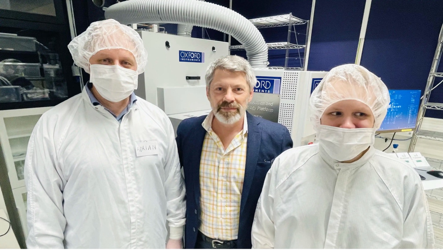
At the recently inaugurated WISE Atomfab at Albanova, researchers can produce extremely thin films and control their composition and structure with very high precision. WISE Atomfab is part of Albanova Nanolab (ANL), and the latest addition to the infrastructure is equipment for advanced ALD (atomic layer deposition), a technique that allows researchers to build up materials layer by layer. The films can be just a few nanometres thick and, in some cases, even thinner.
The Nanolab has previously been able to produce thin films, but the new equipment also allows researchers to coat three-dimensional structures with material.
“This makes it possible to create new types of chips where thin films can be bent around corners. One example is optical waveguides, where so-called single-photon detectors can be placed on the side or around the structure,” says Erik Holmgren, one of the researchers at the lab.
Using ALD technology, the researchers can also deposit very thin layers of certain materials, particularly superconducting nitrides, using chemical methods.
“Chemical methods allow us to control new parameters, such as film stress, density and crystallinity. When we can control virtually every atomic layer, we can produce thinner and more homogeneous films than before. This is particularly interesting for quantum applications, where properties such as kinetic inductance are highly dependent on the thickness of the material. Ultra-thin films can also exhibit properties that are difficult to achieve, or are completely absent, in thicker films,” Erik Holmgren explains.
By controlling materials on this tiny scale, researchers can create properties that are difficult or impossible to achieve using conventional materials manufacturing.
The lab also houses equipment for CVD, or chemical vapour deposition. Using gases and plasma, among other things, researchers can create thin films with properties that are difficult to achieve using conventional manufacturing methods.
For the researchers at WISE Atomfab, quantum technology is another area of particular interest.
“We will use ALD for superconducting, semiconducting, and insulating materials to be used in quantum technology. When certain materials are made extremely thin, their properties can change in ways that are of interest for quantum devices and circuits.”
Open to researchers from outside KTH
Other areas that can benefit from this advanced technology include photonics, where components that manipulate light need to be manufactured, and materials for energy conversion, such as those used in solar cells. Other potential applications include pharmaceutical manufacturing and catalysts, as was highlighted in presentations by ANL researchers during the inauguration.
WISE Atomfab is fully open to researchers from outside KTH, within the national network of Myfab and the Nordic Nanolab Network. Colleagues come here from the Stockholm University and the Karolinska Institute, regional spinoffs and startups, as well as from industry at large, explains Adrian Iovan, who works at the lab.
“More people could certainly be made aware that this facility exists. I’m very proud of this lab. It’s small but efficient and is turning into something extremely good,” he says.
Representatives from WISE and KTH management attended the opening, including Professors Olle Eriksson, Lars Kloo, Anders Forsgren, Oscar Tjernberg and Carlota Canalias. Teachers and early-career researchers from Albanova Nanolab also presented their projects.
Vladislav Korenivski, professor and director of Albanova Nanolab, gave a tour of the new facility. His vision is for the lab to bring together the tools and processes needed for research and development at the nanoscale, while providing strong support for users and making efficient use of resources.
Text: Anna Gullers, KTH Royal Institute of Technology
25 Sep 2026
What if birch leaves could help power tomorrow’s electronics or improve medical technologies?

24 Sep 2026
The application portal for the AP3 call at WISE will open on 1 December.
24 Sep 2026
For Arun, the WISE program was an opportunity to combine scientific curiosity with real-world industrial challenges.
23 Sep 2026
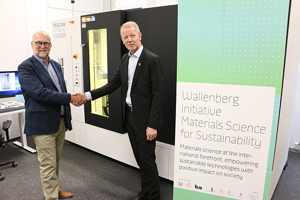
A new advanced instrument for three-dimensional imaging and analysis of materials has been inaugurated at Luleå University of Technology.
21 Sep 2026
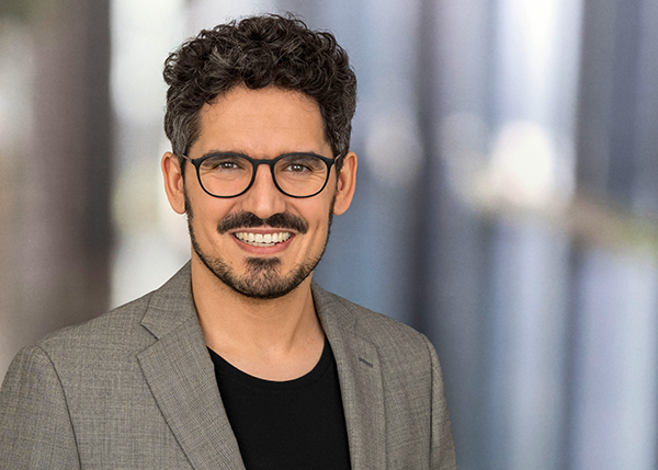
A new research project led by Daniel Weber has received a KAW Proof of Concept (PoC) grant to explore how advanced materials research can be translated into a practical solution for sustainable energy technologies.
18 Sep 2026
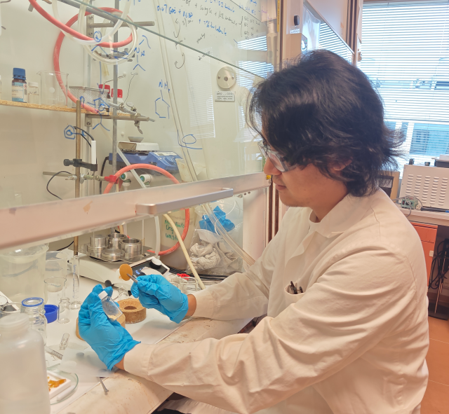
Researchers at Stockholm University developed a method to transform discarded plant material into strong, sustainable packaging. This renewable approach could reduce reliance on fossil-based plastics while using agricultural and forest resources more responsibly.

17 Sep 2026
Don’t miss this lecture on October 1. What will the materials and scientific instruments of the future look like and how can we ensure they contribute to a more sustainable world?

15 Sep 2026
Are you preparing a proposal for WISE-ap3? Make sure you’re fully equipped to meet its strong sustainability ambitions.
15 Sep 2026
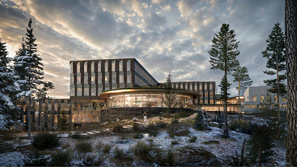
Join us at WISE Networking Days 2026 on November 23-24 in Göteborg!
14 Sep 2026
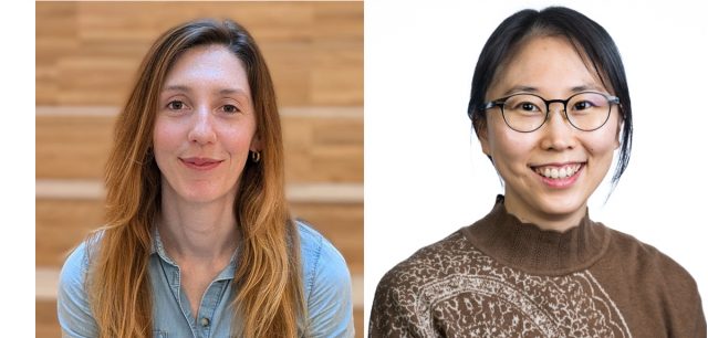
“The WISE Academic Postdoc project gave me my first opportunity to work with a postdoctoral researcher and was an important step in growing my research as an independent PI. The ERC Starting Grant now allows me to build my own research team and pursue a long-term research vision, says Professor Kim from Linköping University.

8 Sep 2026
The call for the Knut and Alice Wallenberg Foundation’s (KAW) Proof of Concept Grants in Materials Science for Sustainability 2026 is now open.
3 Sep 2026
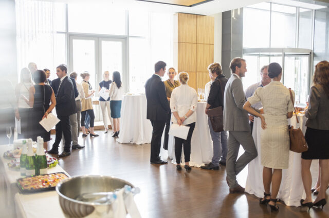
On 18 September 2026, the new WISE ATOMFAB materials fabrication platform at KTH-Albanova Nanolab will be officially inaugurated.
1 Sep 2026
The call for the Knut and Alice Wallenberg Foundation’s (KAW) Proof of Concept Grants in Materials Science for Sustainability 2026 is now open.
26 Aug 2026
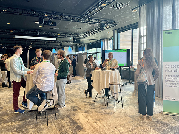
That’s a wrap on Welcome Meeting 2026 – what an amazing event! The Welcome Meeting was a great success, bringing together around 90 participants for an inspiring and engaging day.
26 Aug 2026
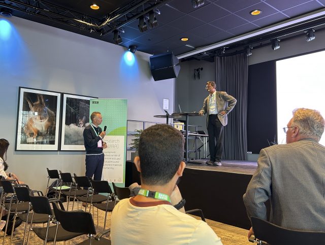
The second day of the WISE Welcome Meeting opened with an inspiring keynote lecture by distinguished Professor Dipankar Das Sarma, who introduced new PhD students and postdocs joining WISE to a fascinating class of materials: halide perovskites.
21 Aug 2026
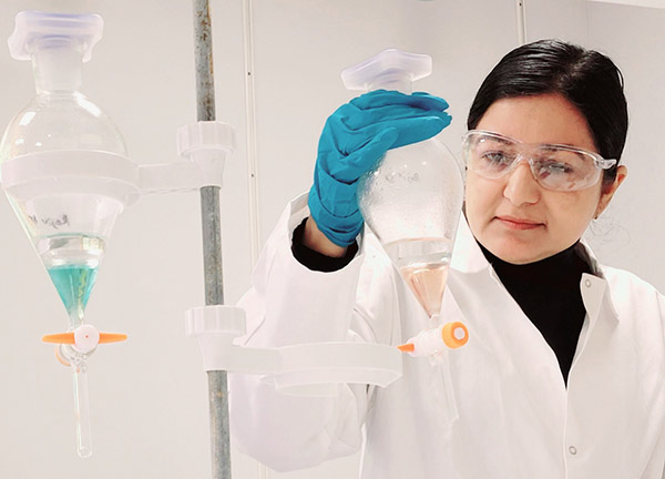
What if yesterday’s waste could power tomorrow’s technologies?
21 Aug 2026
The call for the Knut and Alice Wallenberg Foundation (KAW) Proof of Concept Grants in Materials Science for Sustainability 2026 opens on September 1, 2026.
20 Aug 2026
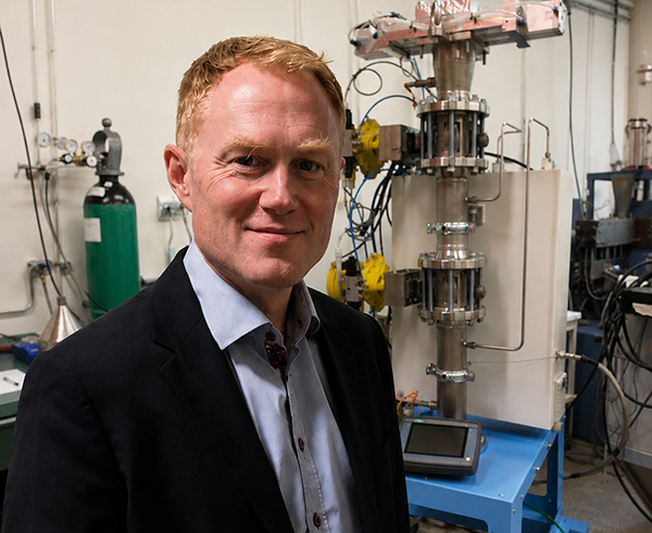
WIRA-SuPRA is a collaborative platform where academia and industry work together to develop the next generation of sustainable plastics and coatings.
19 Aug 2026
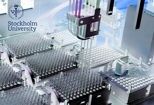
CircuLab is a research infrastructure (Research Technology Platform, RTP) funded by WISE and Stockholm University for the synthesis, processing and application of sustainable materials through integrated AI-driven workflows.

18 Aug 2026
Looking for fresh research perspectives and the opportunity to connect with leading experts? Join us online for the upcoming WISE Invited Professor Lecture on 10 September 2026, from 3:00–4:00 pm […]
18 Aug 2026
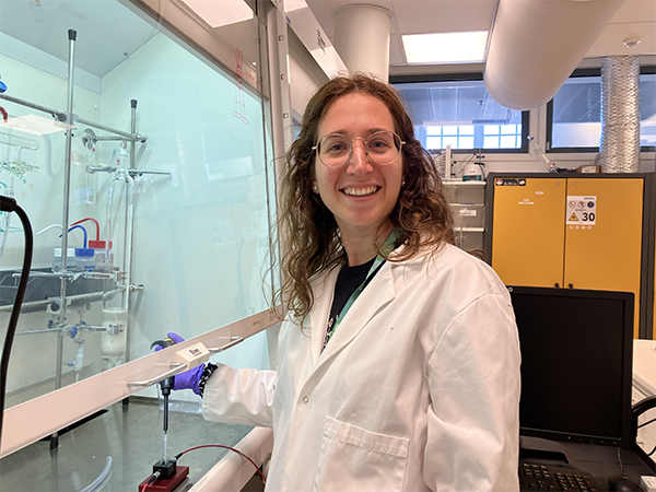
From Italy to Germany and now Sweden, Cecilia Bruschi’s academic journey has been driven by a passion for chemistry and materials research.
17 Aug 2026
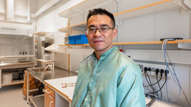
“We ask ourselves not only what is scientifically possible today, but also what advances are needed to bring these technologies closer to commercialization”, says WISE Fellow and Assistant Professor Lizhou Fan from Linköping University.
10 Aug 2026
Jiayao Duan is currently a postdoctoral researcher at Stockholm University, working with Prof. Erica Zeglio. His research is about developing organic electronic materials for bioelectronics, with a growing focus on sustainability and degradability.
7 Aug 2026
What if the next generation of medical implants could safely dissolve in the body once they’ve done their job and be produced with minimal environmental impact?
3 Aug 2026
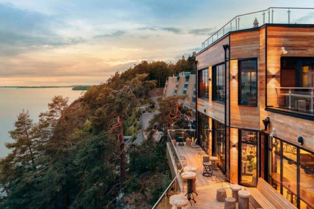
On 24 – 25 August, the WISE Community will welcome its newest members to the WISE Welcome Meeting 2026 at Vildmarkshotellet in Kolmården.
25 Jun 2026
Magnus Berggren, Director of WISE, will assume the role as the Executive Director of Knut and Alice Wallenberg Foundation from 1 January 2027. As a result, he will step down as Program Director of the WISE program and remain at Linköping University on a part-time basis.
23 Jun 2026
“Sustainability is the central theme of my research. Rather than focusing only on performance, we aim to develop technologies that are sustainable from the materials level all the way to manufacturing and end-of-life”, says Magdalena Titirici, Professor at the Imperial College London and WISE Invited Professor.
23 Jun 2026
WISE-affiliated researcher, Professor Ergang Wang at Chalmers University of Technology in Sweden, is coordinating a new EU-funded project, SPECTRA, to develop groundbreaking technologies that use solar energy to transform plastic waste into valuable resources. The project also involves Professor Moyses Araujo at Karlstad University, another WISE-affiliated researcher, as a partner.
22 Jun 2026
Knut and Alice Wallenberg Foundation has increased the searchable framework budget with an additional SEK 265 million to the Wallenberg Initiative Materials Science for Sustainability (WISE), marking a significant expansion of the programme.
12 Jun 2026
Imagine opening a juice box made from materials designed with deeper scientific insight into how they behave at the smallest scales.