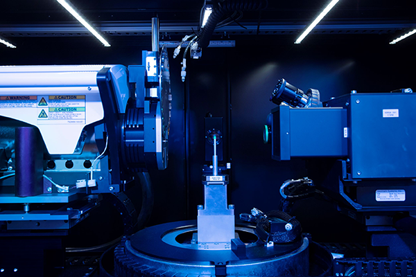
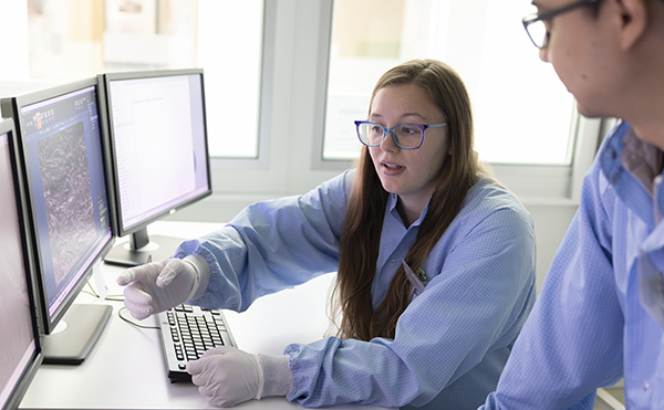
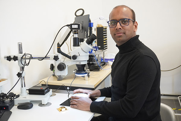
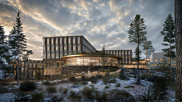
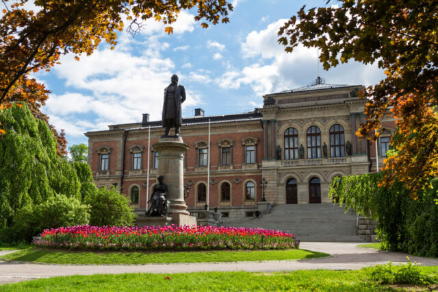
Picture: WISE ACT LUMIA. Picture credit: Luleå University of Technology.
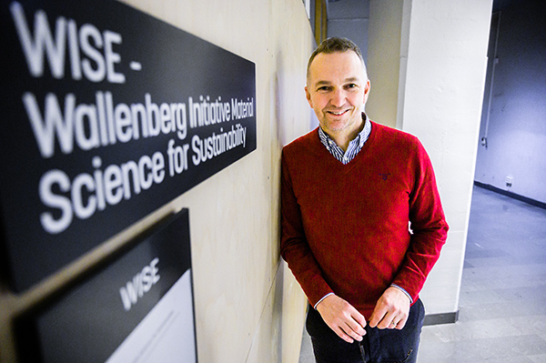
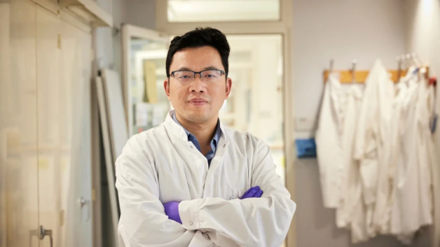
Co-owned by WISE ACT and Wise-EST and hosted at LUMIA (Luleå Material Imaging and Analysis) at Luleå University of Technology, the new FIB SEM lab (and the coming new spectral/dynamic system for x-ray computed tomography) has quickly become a hub for pioneering research.We spoke with Glenn Bark, the scientist in charge of the facility, and Erik Nilsson, chief technician at the FIB SEM lab.
How would you describe the platform’s evolution since its launch, and how has its purpose shifted over time?
Since its official opening in May 2025, the WISE ACT platform has grown from a sophisticated imaging tool into a versatile hub for advanced materials research. Initially, it was known for preparing APT needles, tiny, ultra-sharp samples used to map the position of individual atoms and TEM lamellae, wafer-thin slices that allow scientists to see a material’s internal structure at the atomic level. Now, researchers are increasingly using its correlative workflow between x-ray computed tomography and focused ion beam analysis to perform 3D tomography to explore materials in unprecedented detail, like having X-ray vision that lets you peel back reality layer by layer.
Which early ambitions have you achieved and which goals have grown or changed along the way?
From the start, the platform aimed to give researchers across Sweden access to top-tier tools for both preparing samples and studying materials at the nanoscale. Those ambitions have been realized. Along the way, a new goal emerged: empowering scientists to create visually compelling, deeply informative analyses that make their discoveries resonate not just in labs, but in broader scientific conversations.
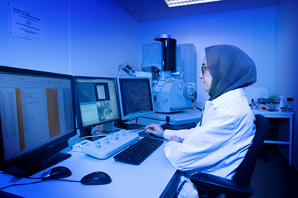
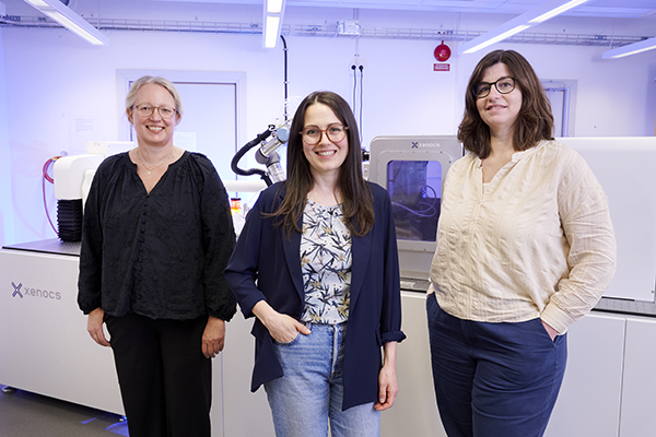
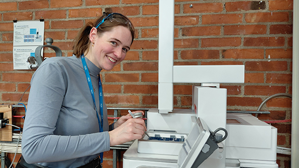
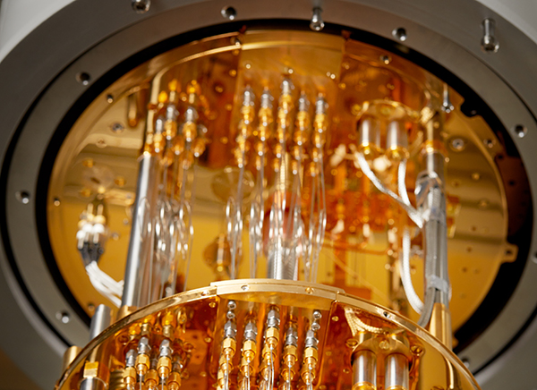
Researcher using WISE ACT LUMIA. Picture credit: Luleå University of Technology.
Research in motion
What kinds of research projects has the platform enabled, and which results or breakthroughs stand out to you?
The platform has been crucial for preparing samples for experiments at MAX IV and PETRA III. In addition, it has also attracted attention from other universities in Sweden, many of which previously lacked the capability to conduct such advanced experiments. The system’s 3D EBSD and EDS capabilities have proven especially valuable, helping researchers uncover details about material structures that were previously inaccessible.
Have any projects led to unexpected discoveries, collaborations, or publications that reached a wider audience?
While only a few publications have emerged so far, given the system has been operational for a short time, multiple projects are underway that promise broader scientific impact. Early feedback suggests that these studies could influence both fundamental research and applied technologies.
Collaboration and networks
How have your collaborations with universities, companies, and public organizations developed?
The platform has strengthened ties with institutions like Chalmers University of Technology, Umeå University, Lund University, and the University of Oulu. Collaborative projects now allow samples and researchers to move efficiently between labs, speeding up discovery and experimentation.
At LTU we have long experience of close collaboration with industry, and this will beneficially spill over into our WISE fellows’ research. They are now working to establish direct collaborations with, for example, LKAB, Boliden, SSAB, Nouryon Pulp and Performance Chemicals. LTU also has an ongoing dialogue regarding WIRA, particularly in areas such as hydrogen and LKAB Reemap, which provides a good foundation moving forward. Overall, there are strong opportunities to further strengthen the connections between our technology platforms WISE ACT@LUMIA and WISE EST, the fellows, WIRA, and industry.
Have new partners or funders joined and influenced the direction of the work?
The Kempe Foundations have funded two postdoctoral researchers dedicated to pushing the limits of the pFIB-SEM system, which is a super-precise “microscope and nano-scalpel” combo used by scientists to look inside materials layer by layer at extremely tiny scales.
Their work will focus on 3D imaging and ToF-SIMS analysis while also helping other groups make the most of the platform’s capabilities. It’s a technique used to figure out what a surface is made of atom by atom and molecule by molecule, by detecting its chemical composition.
Impact and influence
What impact has the platform had on its research field and on society more broadly?
Though it’s been fully operational for less than a year, the platform is already sparking interest in advanced material characterization. Its presence at LTU is strengthening Sweden’s research ecosystem and encouraging the use of cutting-edge imaging techniques.
Has the work contributed to new innovations, methods, or policy discussions?
Researchers are exploring ways to support external users, including legal, insurance, and institutional considerations. The possibility of remote operation is also being discussed, allowing scientists to analyze samples from their home labs while sending the material to LTU for imaging.
Personal reflections
Which moments or developments have surprised you the most?
The enthusiastic response from researchers across Sweden has been especially encouraging. The platform’s appeal extends beyond its specific capabilities; it’s seen as a gateway to a broader set of analytical tools.
What achievement are you personally most proud of and is there anything you would approach differently if you could go back to launch day?
Visits to WISE-affiliated universities have paid off in tangible ways, fostering collaborations and clarifying sample workflows. These efforts have directly increased the number of external projects and strengthened the platform’s role as a national resource for material science.
Side bar: Making the Science Accessible
pFIB-SEM
Plasma Focused Ion Beam-Scanning Electron Microscope
Think of it as a super-powerful microscope that can also “slice” materials extremely thin, layer by layer, to see inside them. Perfect for creating tiny samples and exploring their 3D structure.
TEM Lamellae
Thin slices for Transmission Electron Microscopy
These are wafer-thin pieces of material. thinner than a human hair, that let electrons pass through. This allows scientists to see the internal structure of materials at an atomic level.
APT Needles
Atom Probe Tomography samples
Tiny, needle-shaped samples, sharper than a pinhead, used to map out where every single atom sits in a material. It’s like creating a 3D map of a material, atom by atom.
Available detectors on the FIB SEM
EBSD-Electron Backscatter Diffraction
A technique used in a scanning electron microscope (SEM) to determine:
- Crystal structure
- Crystallographic orientation
- Grain size and boundaries
- Phase identification
EDS (or EDX)-Energy‑Dispersive X‑ray Spectroscopy
Also used in an SEM (or TEM), this technique detects characteristic X-rays emitted by a sample to determine:
- Elemental composition
- Distribution of elements (mapping)
- Impurity detection
ToF‑SIMS-Time‑of‑Flight Secondary Ion Mass Spectrometry
This technique is incredibly sensitive to the very top layer of a material (ca 10 nanometer). It can:
- Identify both whole molecules and their broken fragments
- Create detailed chemical “maps” showing where different substances are located
- Gradually dig deeper into the material to see how composition changes with depth
Because of this, it’s especially useful for studying things like plastics, ultra-thin coatings, organic materials, computer chips, and even tiny traces of contamination.