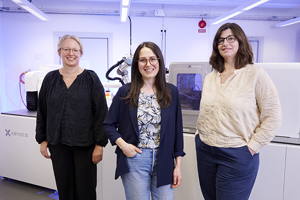
In a recent article in the journal of Advanced Science, Erica Zeglio, a WISE Fellow at Stockholm University, alongside colleagues from the Royal Institute of technology and Stockholm University, achieved ground-breaking precision patterning of polymers at the microscale using high-throughput femtosecond direct laser writing.
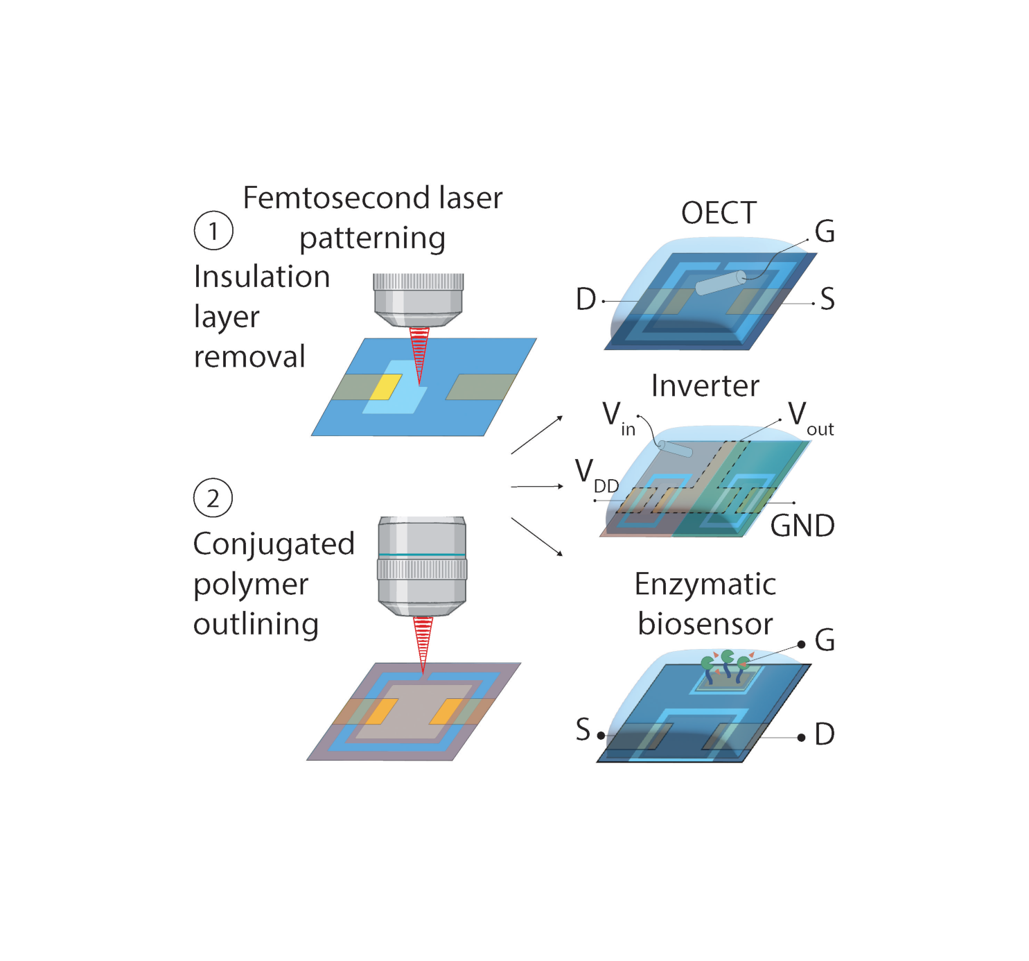
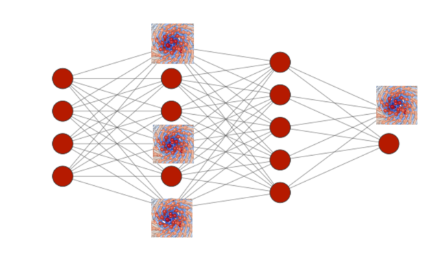
[The figure in the excerpt shows a schematic overview of the OECT manufacturing process using femtosecond pulsed laser writing].
Polymers are important in bioelectronics and flexible electronic devices used for various purposes such as monitoring tissues/cells, health and environmental sensors. Among these devices, the organic electrochemical transistor (OECT) is at the forefront of applications that require low power and amplification of small signals, such as biosensors, wearables, and neuromorphic computing.
OECT fabrication often demands micrometer or even sub-micrometer resolution. Traditional approaches require intricate, time-consuming, multi-step procedures carried out in energy-intensive cleanroom environments. Direct laser writing, however, achieves resolution limits as low as 2 µm without a cleanroom environment, making prototyping and manufacturing much simpler.
Currently, the time and costs involved in developing new prototypes hinder the widespread of OECT-based technology. The research team demonstrated that direct laser writing offers remarkable flexibility and rapid writing speed, facilitating various device architectures and designs, such as logic inverters and enzymatic biosensors.
-Ultrafast direct laser writing opens new possibilities for the rapid prototyping and scaling of microscale devices for bioelectronics. This breakthrough promises to substantially advance the field by simplifying the fabrication process and accelerating innovation,” states Erica Zeglio, Assistant Professor at Stockholm University and WISE Fellow.
The researchers believe that combining this method with advancements in cleanroom-free metal electrode deposition techniques and automated machine vision will pave the way for efficient prototyping and scalable manufacturing of OECTs for bioelectronics applications.
WISE Fellow
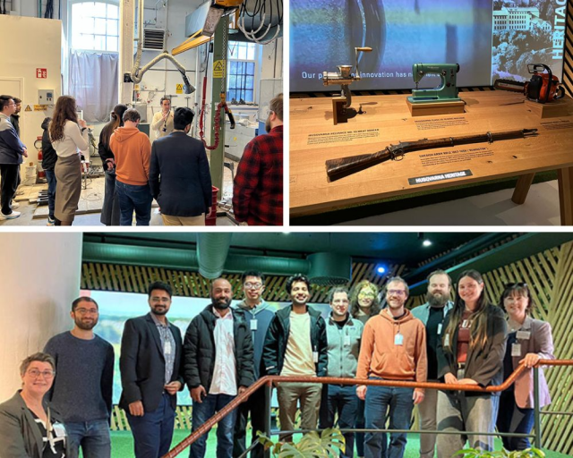
Erica Zeglio became a WISE Fellow in 2023 at Stockholm University. Her WISE Fellow recruitment package included funding for two PhD students and two postdocs. Her research is driven by the need for sustainable materials and device designs that provide better performance -with a particular focus on bioelectronic applications- and improving the long-term impact of modern technological products.
Erica Zeglio’s article can be found at: https://doi.org/10.1002/advs.202307042